
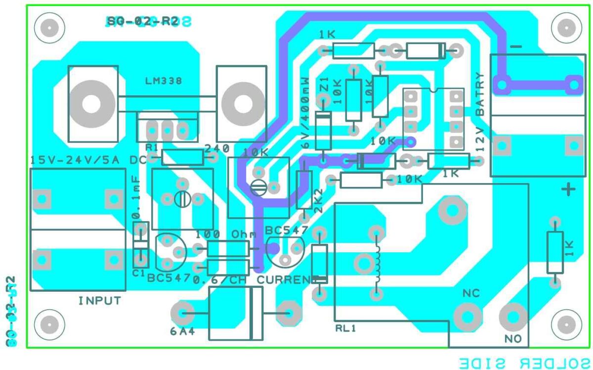
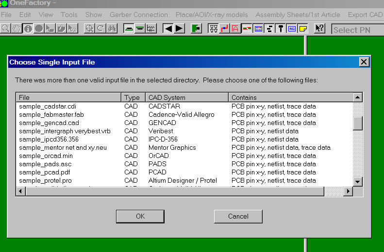

How does a Gerber job file simplify the manufacturing process?
In Stock
$34.99
$29.99
Shipping and Returns Policy
- Deliver to United States » Shipping Policy «
- - Shipping Cost: $5.99
- - Handling time: 2-3 business days
- - Transit time: 7-10 business days
- Eligible for » Returns & Refund Policy « within 30 days from the date of delivery
Find similar items here:
what is gerber file in pcb Informational
- How are they represented differently from the copper pads? What are solder paste stencils and how are they related to Gerber files?
- Via stitching involves placing multiple vias close together to connect different ground or power planes, reducing inductance. The locations of these vias are defined in the drill file. How are fiducials used for layer-to-layer alignment during PCB fabrication?
- Surface finish requirements are typically communicated separately from the Gerber files, often in the purchase order or manufacturing specifications. What are the considerations for generating Gerber files for PCBs with via-in-pad (VIP) technology?
- What role do D-codes play in defining PCB features? What is the difference between RS-274-D and RS-274-X Gerber formats?
- How are multiple PCBs arranged on a single manufacturing panel?
- Keep-out layers define areas where components or copper traces should not be placed. They are often represented as closed shapes in a Gerber file. How are thermal reliefs for component pads defined in Gerber files?
- Smaller and more precise fiducials may be required for fine-pitch components, and their design and placement are defined in the copper layer Gerber files. What is the importance of providing accurate layer stackup details along with Gerber files?
- Heavy copper features require careful design to ensure proper adhesion and manufacturability. Their outlines and connections are defined in the copper layer Gerber files, and the copper thickness is specified in the manufacturing notes. How are fiducials used for step-and-repeat panelization and how are their locations defined in the Gerber files for the panel?
- Edge plating requires specifying which edges need to be plated and the extent of the plating. This is typically indicated in the board outline Gerber file and detailed in the manufacturing notes. What are the considerations for generating Gerber files for PCBs with embedded heat spreaders?
- How does the manufacturer know the physical dimensions and shape of the PCB?
-
Next Day Delivery by USPS
Find out more
Order by 9pm (excludes Public holidays)
$11.99
-
Express Delivery - 48 Hours
Find out more
Order by 9pm (excludes Public holidays)
$9.99
-
Standard Delivery $6.99 Find out more
Delivered within 3 - 7 days (excludes Public holidays).
-
Store Delivery $6.99 Find out more
Delivered to your chosen store within 3-7 days
Spend over $400 (excluding delivery charge) to get a $20 voucher to spend in-store -
International Delivery Find out more
International Delivery is available for this product. The cost and delivery time depend on the country.
You can now return your online order in a few easy steps. Select your preferred tracked returns service. We have print at home, paperless and collection options available.
You have 28 days to return your order from the date it’s delivered. Exclusions apply.
View our full Returns and Exchanges information.
Our extended Christmas returns policy runs from 28th October until 5th January 2025, all items purchased online during this time can be returned for a full refund.
No reviews yet. Only logged in customers who have purchased this product may leave a review.