


Having a glossary of terms can be helpful for understanding Gerber file documentation. What are the different types of PCB layers and how are they represented in Gerber files?
In Stock
$34.99
$29.99
Shipping and Returns Policy
- Deliver to United States » Shipping Policy «
- - Shipping Cost: $5.99
- - Handling time: 2-3 business days
- - Transit time: 7-10 business days
- Eligible for » Returns & Refund Policy « within 30 days from the date of delivery
Find similar items here:
what is gerber file in pcb Informational
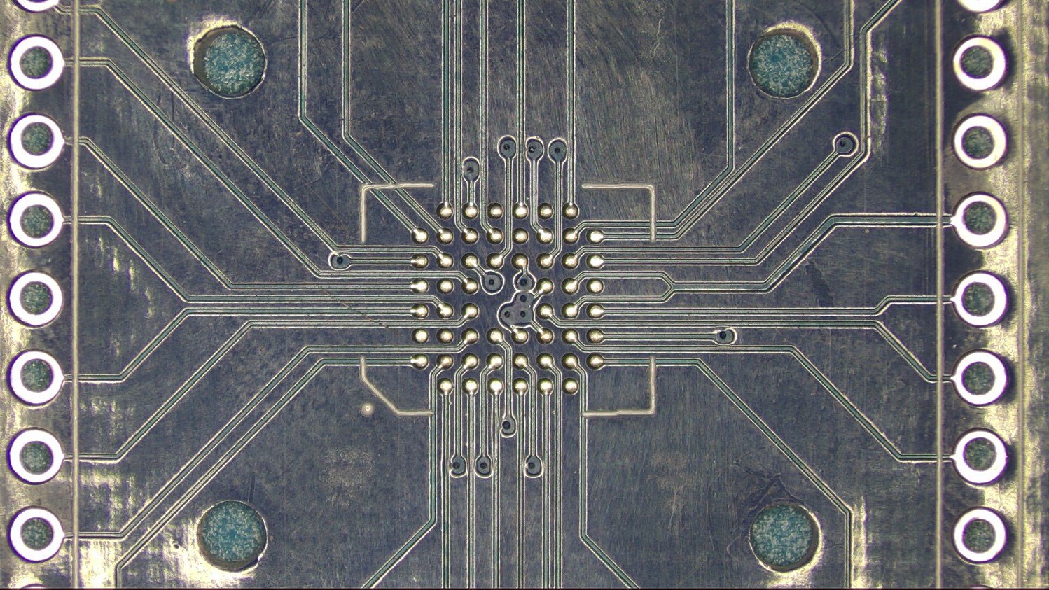
- Test points for ICT are specific pads designed to be contacted by test probes. Their locations are defined in a copper layer Gerber file, and their purpose is often indicated in a separate test point report. What is the role of the assembly drawing in guiding the component placement process, and how does it relate to the Gerber and pick-and-place files?
- How do these notes relate to the Gerber files? What are the considerations for intellectual property protection when submitting Gerber files?
- Fiducial shape and size are important for accurate recognition by assembly equipment. Circular fiducials are common. Their dimensions and locations are precisely defined as copper features in the relevant layer Gerber files. What are the considerations for generating Gerber files for PCBs with mixed signal (analog and digital) circuitry, where isolation and grounding are critical?
- Global fiducials are placed on all layers of the PCB to ensure accurate alignment during the photolithography process. Their locations are consistent across all relevant Gerber files. What is the significance of the Excellon drill format for specifying drilled holes in PCBs?
- Counterbores and countersinks are special types of drilled holes that require specific dimensions and may be indicated in the drill file or a mechanical layer. How are test coupons or impedance test structures included in the PCB design and Gerber files?
- Why are soldermask openings necessary for soldering?
- What is the process of converting Gerber files into a physical PCB?
- The type of solder mask is usually specified in the manufacturing notes or purchase order. While the Gerber files define the openings in the solder mask, the type of mask material and application process are separate considerations. What are the considerations for generating Gerber files for PCBs with buried resistors or capacitors?
- Controlled impedance test coupons are specific trace structures designed to allow manufacturers to measure the impedance of transmission lines on the fabricated PCB. Their layout is included in the relevant copper layer Gerber files. What is the process of design for assembly (DFA) and how does it influence Gerber file generation (e.g., silkscreen information, component pad design)?
- How do manufacturers interpret the information for these internal connections?
-
Next Day Delivery by USPS
Find out more
Order by 9pm (excludes Public holidays)
$11.99
-
Express Delivery - 48 Hours
Find out more
Order by 9pm (excludes Public holidays)
$9.99
-
Standard Delivery $6.99 Find out more
Delivered within 3 - 7 days (excludes Public holidays).
-
Store Delivery $6.99 Find out more
Delivered to your chosen store within 3-7 days
Spend over $400 (excluding delivery charge) to get a $20 voucher to spend in-store -
International Delivery Find out more
International Delivery is available for this product. The cost and delivery time depend on the country.
You can now return your online order in a few easy steps. Select your preferred tracked returns service. We have print at home, paperless and collection options available.
You have 28 days to return your order from the date it’s delivered. Exclusions apply.
View our full Returns and Exchanges information.
Our extended Christmas returns policy runs from 28th October until 5th January 2025, all items purchased online during this time can be returned for a full refund.
No reviews yet. Only logged in customers who have purchased this product may leave a review.